
Home > Industry Information > Founded Only 3 Years Ago, This Company’S New Lithography Machine Claims To Be Comparable To ASML EUV
Recently, Substrate, a three-year-old startup in the United States, announced that it has successfully developed a lithography machine with performance comparable to ASML EUV.
This company was founded in 2022 with a team size of only about 50 people.Its engineers said: In the process of realizing independent chip manufacturing, the first core problem to be overcome is photolithography technology.The ultimate goal is to get TSMC and ASML out of the market.
According to reports, Substrate uses a new photolithography method.Its equipment generates short-wavelength X-ray light sources through particle accelerators, which can form thinner beams and print 12nm patterns. Its performance is close to the current most advanced High-NA EUV lithography machine.
You know, an ASML High-NA EUV lithography machine sells for more than 400 million US dollars, and Substrate’s solution aims to achieve lower cost and smaller size.
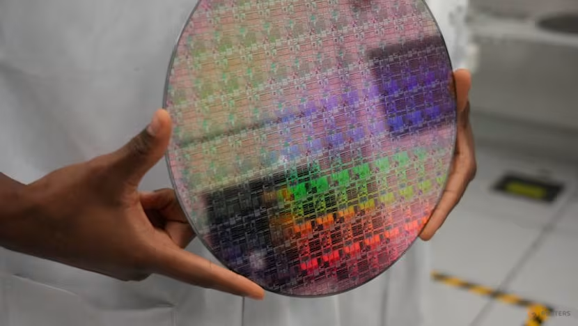
Source: Jim Wilson/Pool via REUTERS
According to data disclosed by the company, this X-ray lithography equipment has partially overcome the technical bottleneck that has long plagued the industry. Its performance is as follows:
Single exposure of all layers possible at 2nm, 1nm and possibly beyond nodes;
Resolution comparable to high numerical aperture EUV;
12nm features confirmed;
Ability to present complex, arbitrary patterns;
Overlay accuracy ≤ 1.6 nm, full wafer CDU ≤ 0.25 nm, line edge roughness (LER) ≤ 1 nm, LCDU ≤ 1.5 nm;
Advanced wafer production costs will be 50% lower than current solutions.
If these data are true, this technology is expected to approach or even surpass ASML’s latest EUV equipment in performance while significantly reducing manufacturing costs.
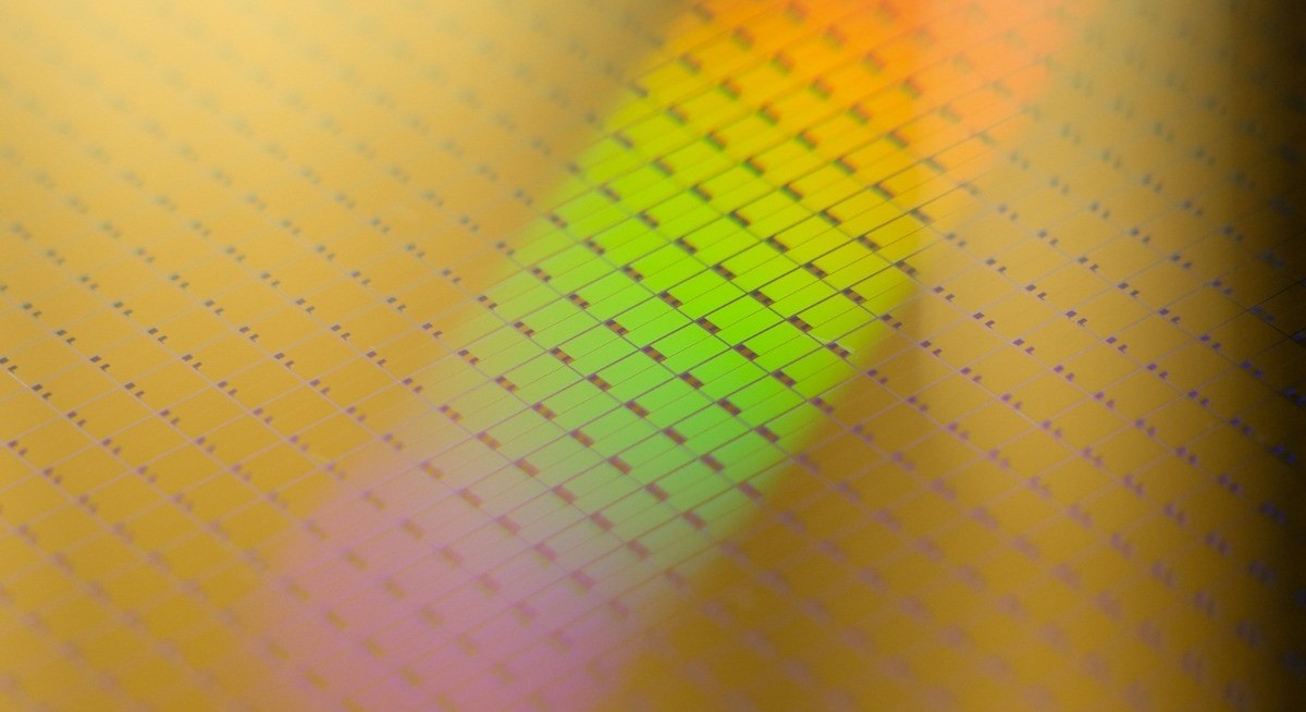
Source: theedgesingapore
Substrate said that the photolithography machine is only the first step in the company's plan.The next step is to establish domestic wafer manufacturing capabilities in the United States, enter the wafer foundry field, and compete directly with TSMC.
The company hopes to further lower the threshold for chip manufacturing by using photolithography machines that cost far less than existing ones.
Currently, Substrate has received more than US$100 million in financing, and the company’s valuation has reached US$1 billion.However, the industry generally believes that there are still huge challenges to achieve mass production.
Advanced process research and development often requires billions of dollars in investment, and the cost of building an advanced wafer fab is as high as more than 15 billion U.S. dollars, and requires long-term manufacturing experience and process accumulation.
For giants such as Intel and Samsung, it is still difficult to perfect this type of process, and Substrate's goal is equally difficult.
Sources of news data: "Reuters", "Bloomberg", theedgesingapore
Industry Information


© ShanHai Chip City (Shenzhen) Technology Co., Ltd. Guangdong ICP No. 2024259560 Guangdong Public Security No. 44030402005948

