
Home > Industry Information > SD NAND Vs Traditional Storage: Compatibility, Stability And Ease Of Use Analysis
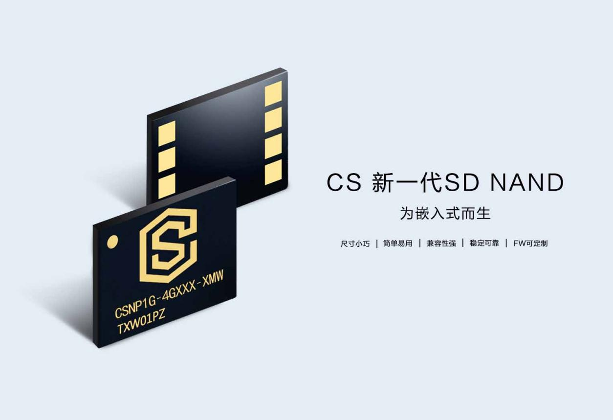
I don’t know if you have used the above SD NAND. I have recently used Brontosaurus SD NAND. I found that SD NAND has many advantages over other storage products.
[1Gb SD NAND Second Generation] Product Purchase Link
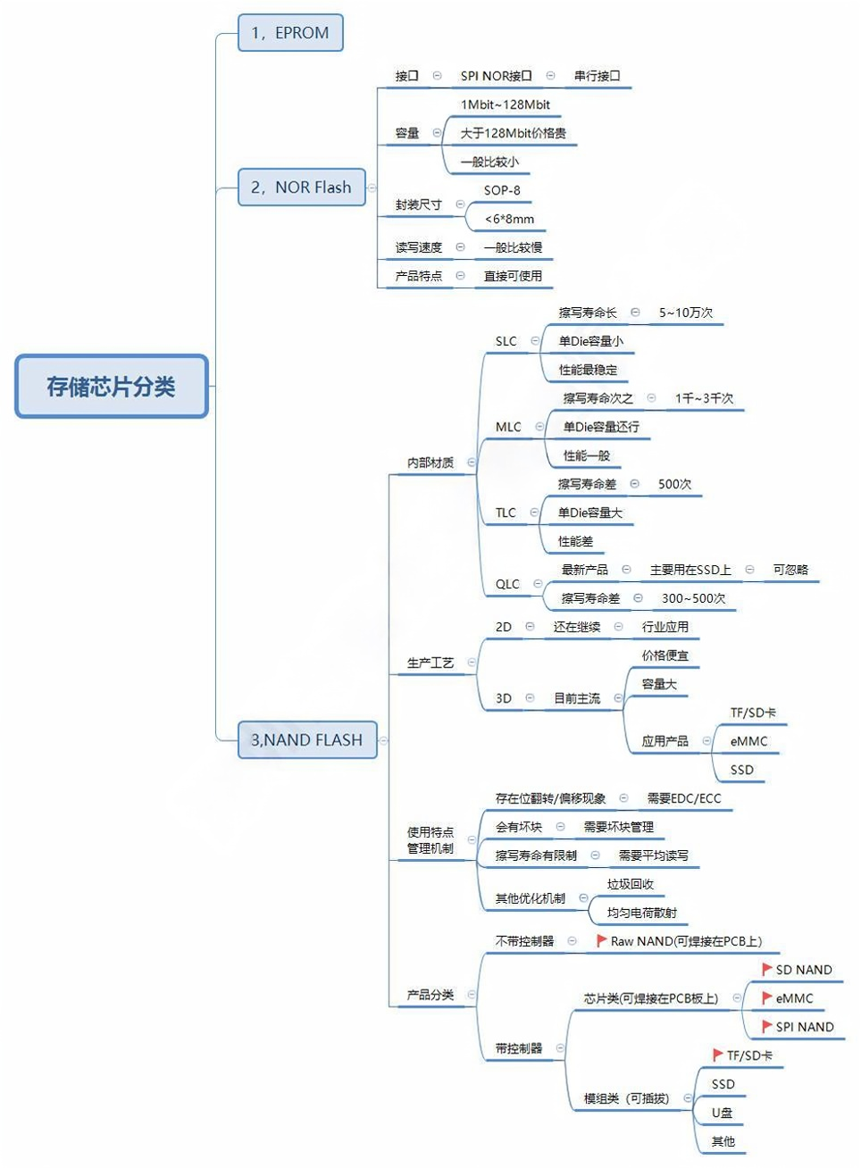
We roughly divide storage products into three categories: E2PROM, NOR, and NAND. Their framework is as follows: (The picture below is from the Brontosaurus company blog)
1. E2PROM
The capacity is very small and currently exists inside some MCUs, remote controls, electric fans and other small household appliances.Used to store some basic information.Users basically don't care about this.Therefore no detailed description is given here.
2. NOR Flash
It is currently the most widely used memory chip. It is basically used in mainstream electronic products.It is even used inside the camera of our mobile phones and on the screen driver circuit board.Mainly used to store code and some smaller data files.The mainstream is SPI NOR interface; Mainstream capacity: 1Mbit~128Mbit; Package: mostly SOP-8, some smaller; sizes are also relatively small.NOR The Flash architecture determines that its capacity cannot be increased, and its reading speed is relatively slow.The advantage is that it is relatively simple and easy to use.You can even access the data directly using the address without setting up a file system.
3. NAND Flash
The most popular memory chip at present.Because it is involved in the electronic products we often use in our lives.For example, if you buy a mobile phone, will you definitely consider 64GB or 256GB?When buying a laptop, should I buy a 256GB or 512GB hard drive?(Currently, most computers use NAND-basedSolid state drives for Flash products).
【4Gb SD NAND Second Generation】Product purchase link
Through my own use, consulting a large amount of storage data, and simple hardware transmission speed testing, we can conclude that the advantages of CS SD NAND are as follows:
Internal material
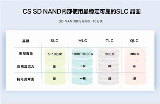
NAND FLASH can be divided into SLC/MLC/TLC/QLC in terms of material. The essential difference is how many bits of information can be stored in the smallest storage unit.SLC(2bit)/MLC(4bit)/TLC(8bit)/QLC(16bit). In this way, the storage density of the wafer will be doubled.The characteristics of these four wafers are as follows:
Production process
The biggest benefit brought by the current production process and upgrading to 3D is the N-fold increase in storage density.In recent years, the mainstream capacities of mobile phones and notebooks have become larger, which is directly related to the use of 3D technology in the industry.
Usage features/management mechanisms
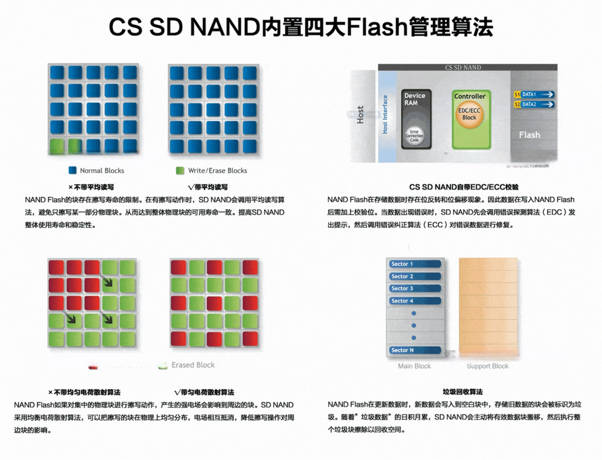
NAND Flash products themselves have certain characteristics. To be used normally, they must be equipped with corresponding management mechanisms.The main ones are:
1. NAND Flash has bit flips and bit offsets.The data originally stored is 0101, but there is a certain probability that it will become 1010.At this time, you need to equip an EDC/ECC mechanism;
2. NAND Flash will have bad blocks when it leaves the factory (don’t be surprised, it will be marked when it leaves the factory, and the proportion is very low), and bad blocks may also occur during use.Therefore, it is necessary to equip dynamic and static bad block management mechanisms;
3. NAND Flash has a writing life limit.Each block has a write life.Therefore, it is necessary to equip an average read and write mechanism.Let the overall blocks be used in a balanced manner;
4. NAND Flash is erased first and then written. The strong current of concentrated erasing and writing will have an impact on surrounding blocks.It needs to be equipped with garbage collection, balanced charge scattering mechanism, etc.
CS Genesis SD NAND integrates these algorithms internally.The schematic diagram is as follows:
Products
Chip products include SD NAND, eMMC, and SPI NAND. Their common feature is that they all have internal management mechanisms for NAND Flash.Relatively speaking, it can reduce the load on the CPU.The exception is SPI NAND, which only has some internal management algorithms, so it still needs to write a driver.The mainstream module products include TF/SD cards, SSD, USB flash drives, etc.
[32Gb SD NAND Second Generation] Product Purchase Link
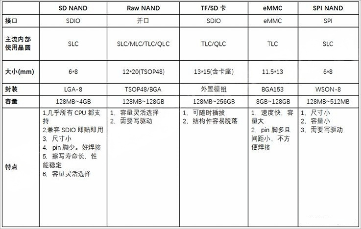
Let’s make a simple comparison of several commonly used products:
NOR vs. NAND comparison
1. NOR Flash supports random access, so it supports XIP (execute In Place). NAND Flash needs to be read in blocks, so it does not support XIP.
2. The theoretical reading speed of NAND FLASH is similar to that of NOR Flash. The actual situation will vary depending on the interface.
3. Both NOR and NAND need to be erased before writing. NOR is erased in blocks of 64 to 128KB, and it takes about 5 seconds to perform a write/erase operation. NAND is erased in blocks of 8 to 32KB, and it takes about 4ms to perform a write/erase operation.
4. NAND has more theoretical maximum erase times than NOR.
5. NOR driver is simpler than NAND. NAND FLASH needs to communicate with the Host through a special NFI (NAND FLASH Interface), so the driver is relatively complicated.
6. All Flash will have bit reversal problems. The probability of NAND bit reversal is higher than that of NOR. NAND Flash must use ECC.
7. The unit size of NAND is almost half that of NOR devices, so the cost of NAND is lower.
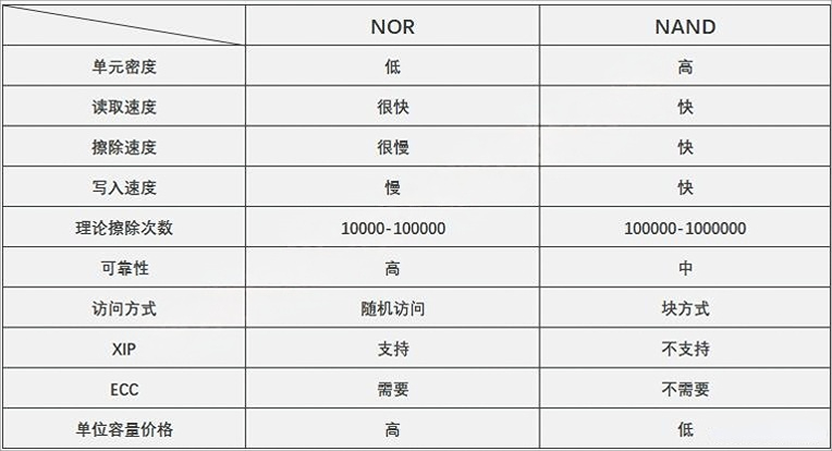
NOR and NAND have their own characteristics, with different application scenarios and application difficulties. SD NAND retains the high-quality features of the NAND architecture while improving its shortcomings. The built-in controller can manage NAND Flash by itself. Users do not need to handle ECC and bad block management externally. The MTD layer is eliminated, and users do not need to write cumbersome driver code.These features also make it possible for NOR users to upgrade NAND.
After comparing the architecture, let’s take a look at the product comparison:
Comparison between CS brand SD NAND and SPI NAND
1. Similarities:
Internal material:The mainstream basically uses SLC NAND Flash wafers, which have a write and erase life of 5 to 10W times.
Package size:The mainstream sizes are 6*8mm, 8pin.
2. Differences:
The interface is different:SD NAND is normally connected to the SDIO of the CPU. Some platforms also support SD NAND to be connected to the SPI interface (but the read and write speed may be slower); SPI NAND is connected to the SPI interface, but cannot be used normally when connected to SDIO.
Driver:Basically, mainstream CPU platforms come with SDIO drivers, so SD NAND does not require users to write additional drivers; in addition, SD NAND has built-in EDC/ECC, bad block management, average read and write, garbage collection and other algorithms for NAND Flash.The management of NAND Flash is completely done; while SPI NAND is mainly for protocol conversion, from parallel port to SPI interface. Some manufacturers' products have built-in EDC/ECC algorithms, but other management mechanisms are not included.As a result, users still have to write drivers when using SPI NAND.
Reading and writing speed:Due to differences in interfaces and protocols, the speed difference between the two is relatively large.SD NAND uses 4-bit transmission bandwidth, and its read and write speeds are much faster than SPI NAND. The maximum write speed can reach Class 10 level; while SPI NAND is still mainstream in 1-bit transmission mode, and its read and write speeds are much slower.
Stability:SD NAND due toIt has a full set of management algorithms built-in, which will be much better in terms of stability.Especially for power failure protection.For example, the second generation of CS brand SD NAND passed the customer's 10K times random power-off test.Both SPI NAND and Raw NAND inherit the disadvantages caused by the erase-before-write mechanism of NAND Flash. It is easy to lose data when the power is suddenly lost while writing data.
Overall, SD NAND is a Total Solution that integrates a complete NAND Flash algorithm, while SPI NAND mainly completes protocol conversion, and the built-in algorithm is incomplete.
cs brand sd nand summary
1. Strong compatibility.Basically, if the customer main control can use TF card and SD card, it can use SD NAND.If you change the main control to a new one, as long as the new main control has an SD interface, you can basically use SD NAND Flash.
2. Small size and stable welding.It is a WSON-8 package with a size of 6x8mm.Fewer PINs and smaller size can not only save PCB board area and reduce costs, but also make the final product smaller.
3. Suitable capacity.The current mass production capacities are 128MB and 512MB, and SD NAND with 1GB and 4GB capacities will be launched later.Customers can choose the appropriate capacity according to their actual needs and reduce costs.
4. Simple and easy to use.SD NAND has built-in bad block management, average read and write, dynamic and static EDC/ECC algorithms, etc. In addition to making the quality of the product more stable, better extending the life, and reducing the load on the CPU.All subsequent operations on NAND Flash can be handed over to SD NAND, and the CPU no longer needs to take care of it.My boss no longer has to worry about my NAND Flash driver.
5. Long service life and stable performance.SLC NAND is the type with the longest service life and the most stable performance among NAND Flash.The erase and write life of up to 10W makes SD NAND very durable.
It can be seen that CS brand SD NAND is not only a SMD T card, SMD TF card, SMD SD card, SMD memory card, SMD flash memory card, SMD card, SMD USB disk, and SMD UDP, it can also be said to be the smallest TF card, the smallest NAND Flash product, an easy-to-use NAND Flash product, a NAND Flash product that does not require a write driver, a long-life NAND Flash product, and a stable NAND Flash product.
To sum up, I highly recommend the CS creation brand SD nand.
Industry Information